Circuit Decomposition
Fig 1: Electrosmash Block Diagram of Dunlop CryBaby GCB-95
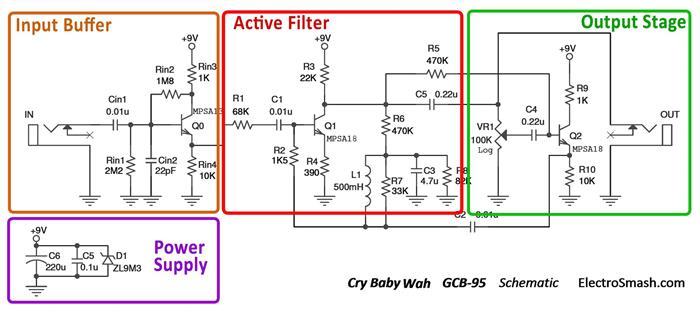
As displayed in figure 1, the Dunlop CryBaby GCB-95 is made up of four essential blocks: an input buffer, filter, output, and power supply. For the purposes of this digital model which makes use of the bilinear transform to model linear components based on their transfer functions, the input buffer and active filter are examined the closest. The 9V source supplies power to the transistors and the zener diode (D1) protects the circuit from voltage peaks. This does not need to be modeled digitally. The output is taken before the variable potentiometer (VR1) so it does not impact the volume. The stage is designed as a buffer for the middle pin of the potentiometer where there is a DC return for feedback loop, resistance to block voltage oscillation, and a transistor that is biased from the 480k resistor (R5).
Fig 2: Input Buffer Schematic and Frequency Response
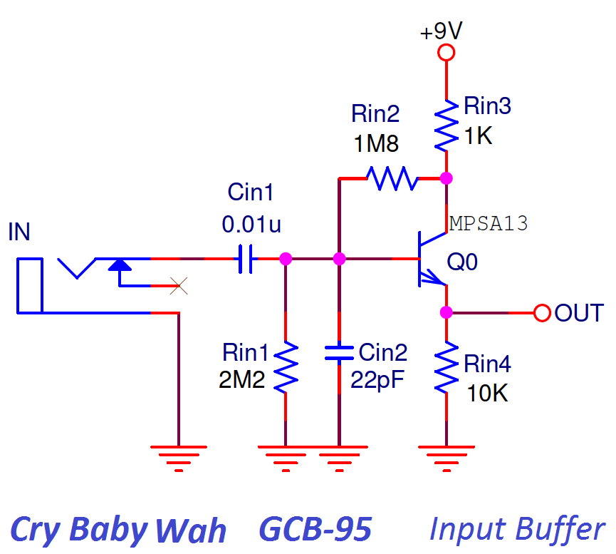
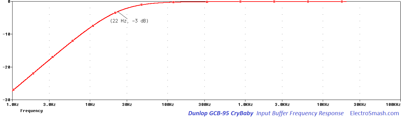
The input buffer has a high input impedance and outputs a low output impedance into the active filter stage. Cin1 blocks DC in addition to Rin1 and Rin2 forming a voltage divider that establishes the resting point (bias) for the transistor Q0. The network has an input resistance of 750kΩ which is used for the digital model in a simplified RC high pass filter. The analog input stage creates a high pass filter with the cutoff frequency at 22 Hz. The approximated transfer function to represent the high pass filter is and with an R1 of 750kΩ and C1 of 0.01µF, the cutoff in the digital model is at 21.22 Hz.
Fig 3: Active Filter Schematic and Frequency Response
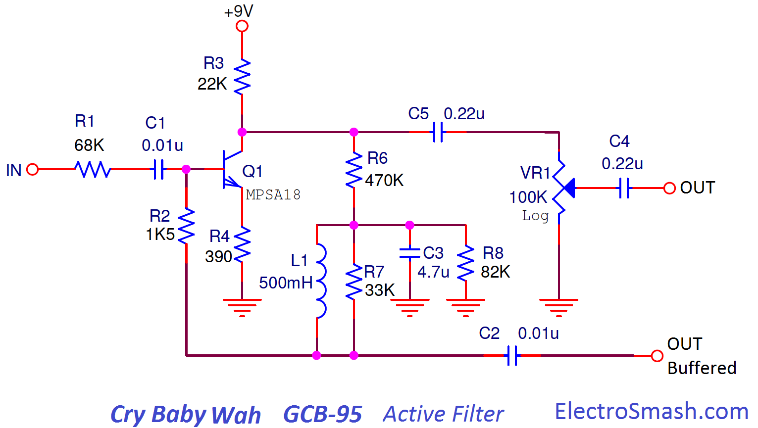
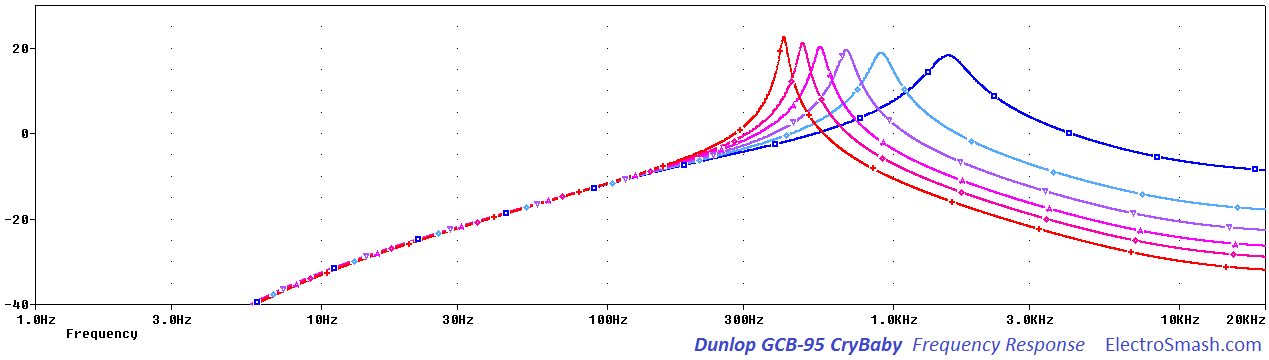
The active filter is the main section that is responsible for creating the audible wah effect that gives the pedal its characteristic. It is also the section that is most commonly modified in order to change the sweep range and Q factor of the filter. C1 operates as a bypass that isolates the previous block. The parallel resistors R7 and R8 set the default voltage that is applied to the transistor and on the inductor. The potentiometer controls the level that feeds the transistor. This is modeled as a gain factor that is divided in the transfer function which causes the center frequency to move. Its transfer function is where the gain scales the output in amplitude and the effective gain controls the center frequency of the filter. The effective gain is derived from the voltage gain inside the transistor stage and from the changes in the potentiometer that determines how the LC resonates. The gain refers to the additional volume gain in the path over C5 and VR1.
Analog to Digital Conversion
Eq 1: Input Buffer Analog to Digital Conversion
Starting with the transfer function
Applying the bilinear transform
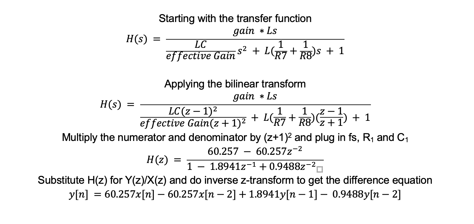
Multiply the numerator and denominator by (z+1) and plug in fs, R1 and C1
Substitute H(z) for Y(z)/X(z) and do inverse z-transform to get the difference equation
Eq 2: Active Filter Analog to Digital Conversion
Starting with the transfer function
Applying the bilinear transform
Multiply the numerator and denominator by (z+1)2 and plug in fs, R1 and C1
Substitute H(z) for Y(z)/X(z) and do inverse z-transform to get the difference equation
Matlab Implementation
Fig 4: Time Animated Frequency Response and Pole-Zero Map and Impulse Response
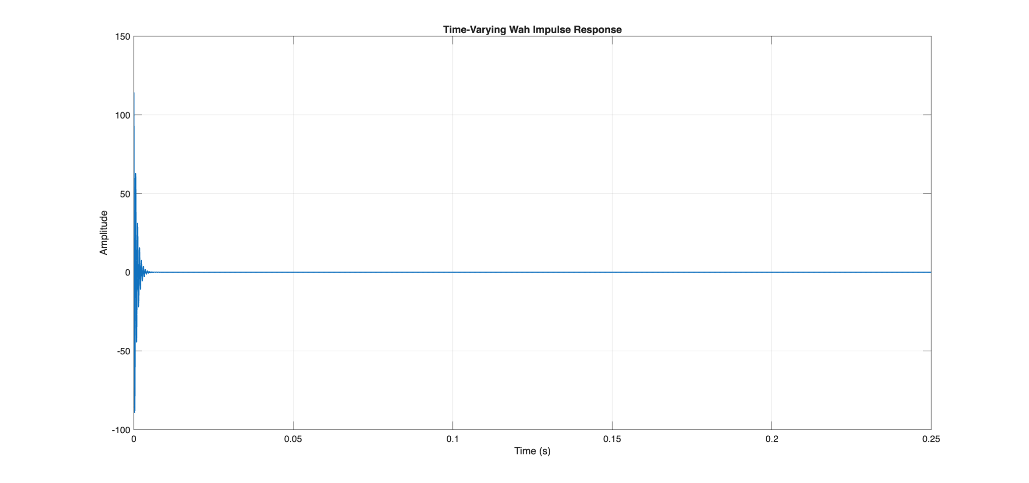
By using the bilinear transform to obtain the digital transfer function and difference equations of the analog systems, the Matlab implementation mainly involved placing the functions inside a process loop that is able to read the mp3 file sample by sample and update the coefficients each time it loops. Additionally the code animates the frequency response and pole-zero plot as the effective gain is oscillated by the variable alpha_vec which is a 0.5 Hz sine wave. Fig. 4 showcases the pole locations moving as the filter oscillates. The blue line shows the analog approximation of the pedal with the transfer function H(s), while the dashed red line shows the digital model with the bilinear transform.
Fig 5: Alpha Modulating the Effective Gain
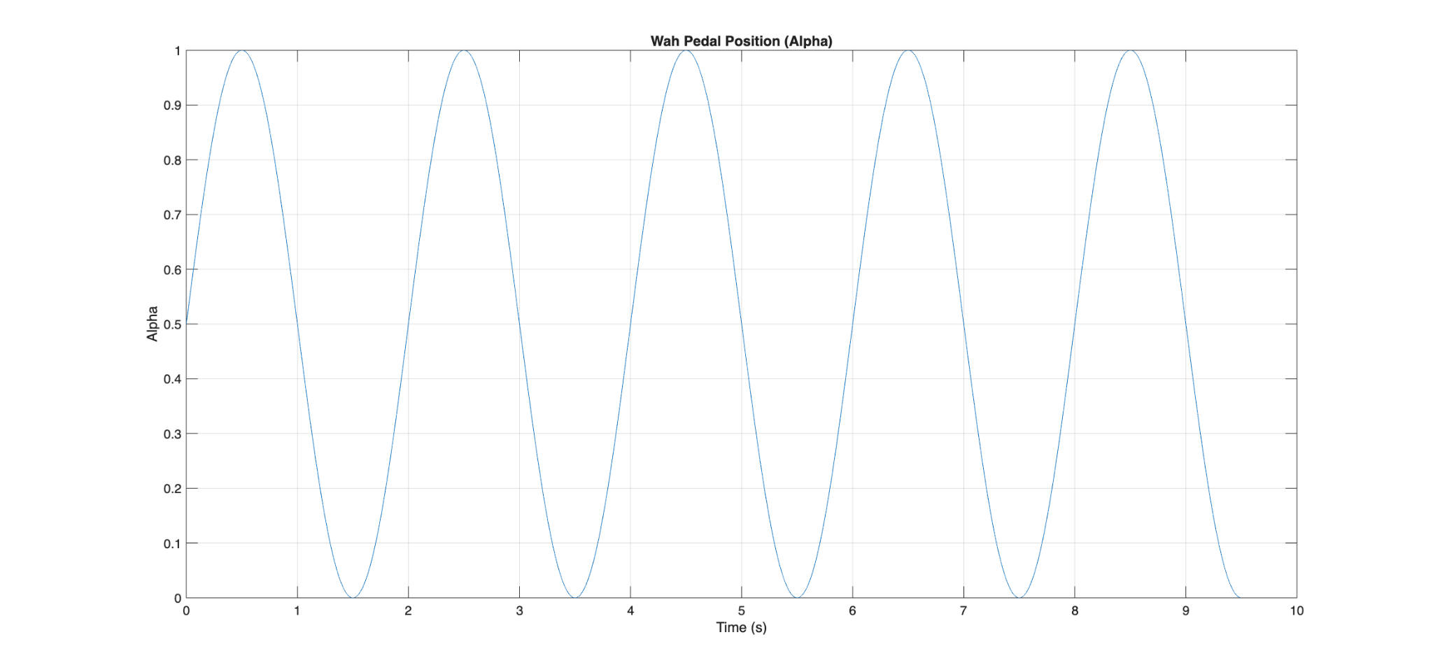
Fig. 5 displays the 0.5 Hz sine wave that modulates the effective gain in order to move the center frequency of the narrowband bandpass filter.
Links to Matlab code and Audio Output
Audio Output:
https://drive.google.com/file/d/1UCim9xUQKaijm2RuqdixKVN189k4iQn-/view?usp=sharing
Matlab Code: https://drive.google.com/file/d/1K7l9UZEcwsa2KrY-9RareTSVXD7nIHat/view?usp=sharing
Electrosmash Source
Electrosmash, and Mikes S. "Dunlop Crybaby GCB-95 Circuit Analysis." ElectroSmash - Electronics for Audio Circuits. Accessed February 20, 2026. https://www.electrosmash.com/crybaby-gcb-95.