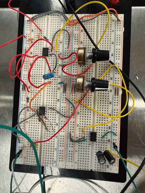
Fig 1: Annotated Schematic
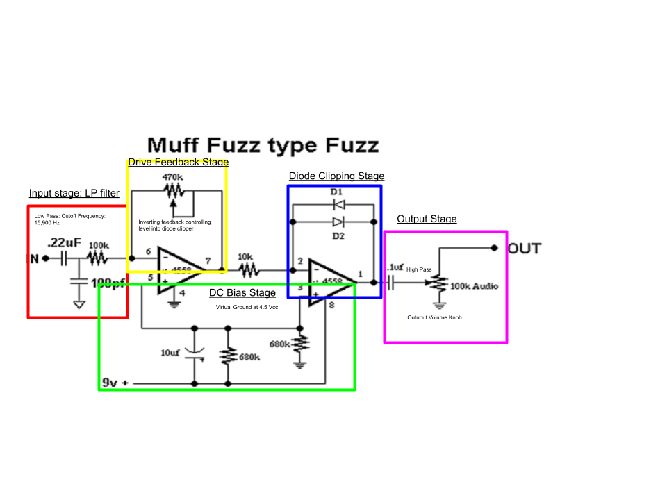
Fig 2: Breadboard Circuit
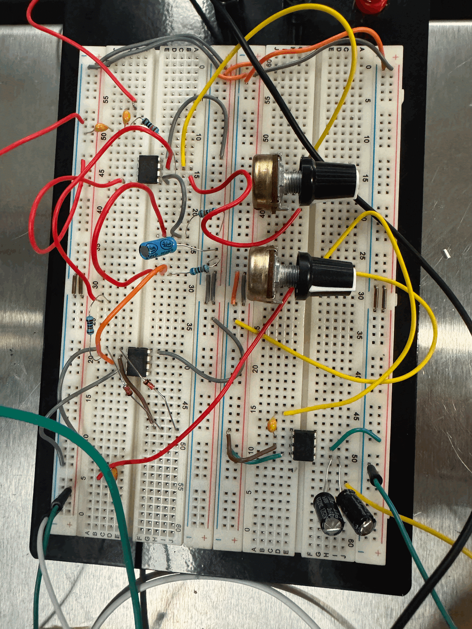
Fig 3: Circuit Schematic
Analysis
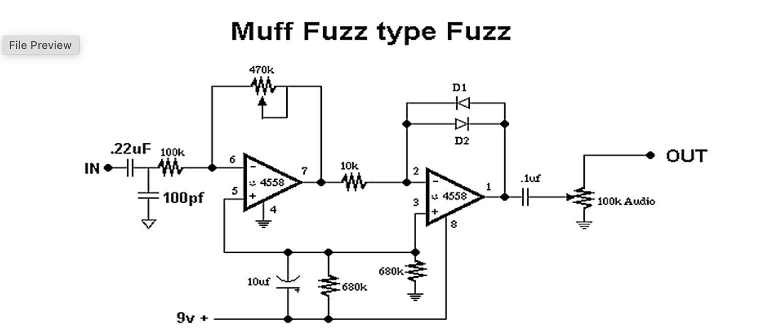
The input starts with a 0.22uF capacitor that blocks dc and goes into a high pass filter with a 100k resistor. This input node starts with high impedance and reduces unwanted noise. This node leads into an inverting amplifier with a 4558 chip. The feedback resistor is attached with a potentiometer to control this first stage of clipping. The output of the inverting amplifier is connected into another inverting operational amplifier with a 10k resistor. For the feedback into the second opamp, there are two diodes in parallel which causes most of the distortion and fuzz. The two diodes being faced in opposite directions make the gain more linear/compressed giving it that fuzz sound instead of just overdrive. The output of the second opamp goes to a capacitor to clean up dc voltage which then goes into another potentiometer with 100k resistance to control the overall output. Both opamps are being supplied by a single 9+volts so it needs a dc bias component. Each positive part of the opamps is both connected to a capacitor with a 10uF and a resistor with 680k ohms to the 9volt power supply. On this same node which both opamps are connected to, there is an additional resistor with the same 680k ohms connected to ground.
Modifications
We tried changing the .22 µF for a smaller value (0.047 µF) which enhanced the fuzz of the low frequencies. The low frequencies seemed to distort much significantly lower on the knob rotation. This isn’t ideal for most fuzz cases as it oversaturates low frequencies but has an interesting use case for low frequency sources where the user might want to add significant gain to low frequencies.
Challenges and Resolution
A major challenge in the process of building the circuit was the organization of the breadboard. Through experimenting with different node setups and accounting for the entire schematic, we were able to achieve a properly partitioned and organized breadboard. The actual issues of our circuit functionality led us to discover we were working with faulty resistors and power supply. The circuit was able to run once we replaced the components.
Individual Reflection
This project helped me deepen my understanding of nonlinearities in circuits and helped me develop my troubleshooting skills. Since this circuit was significantly more complex than any other circuit I have built, it was critical to be careful during the construction of the circuit. When it didn’t work at first, we started by checking every connection and realized that we missed one or two connections. Additionally, we had to test using different component values for the variable resistor and polarized capacitors since we did not have the exact component values. We did not face any issues with the second operational amplifier with the diode clipping and it worked as we expected from the construction of the circuit.